Module degradation | When the phenomenon of so-called snail trails first emerged over a decade ago, they prompted concerns of a major new problem afflicting PV modules. Sylke Meyer, Marko Turek, Thomas Manke, Stephan Großer and Christian Hagendorf, who have contributed extensively to understanding the science behind snail trails, review the latest thinking on the phenomenon and what it means for plant performance More than 10 years ago, the first owners and operators of PV modules reported the appearance of a phenomenon which was unknown and unaccountable at that time. Dark stripes crossing the area or framing the edge of solar cells were observed within a short time (several months) after installation of the modules [1]. The mysteriousness of this defect was increased by the fact that in many cases neither all cells of a module were affected nor all modules of one installation. And it is perhaps due to this initial perplexity that pictorial but misleading names were used to describe the phenomenon: snail trails, snail tracks, worm marks or framing.

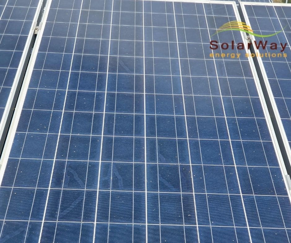
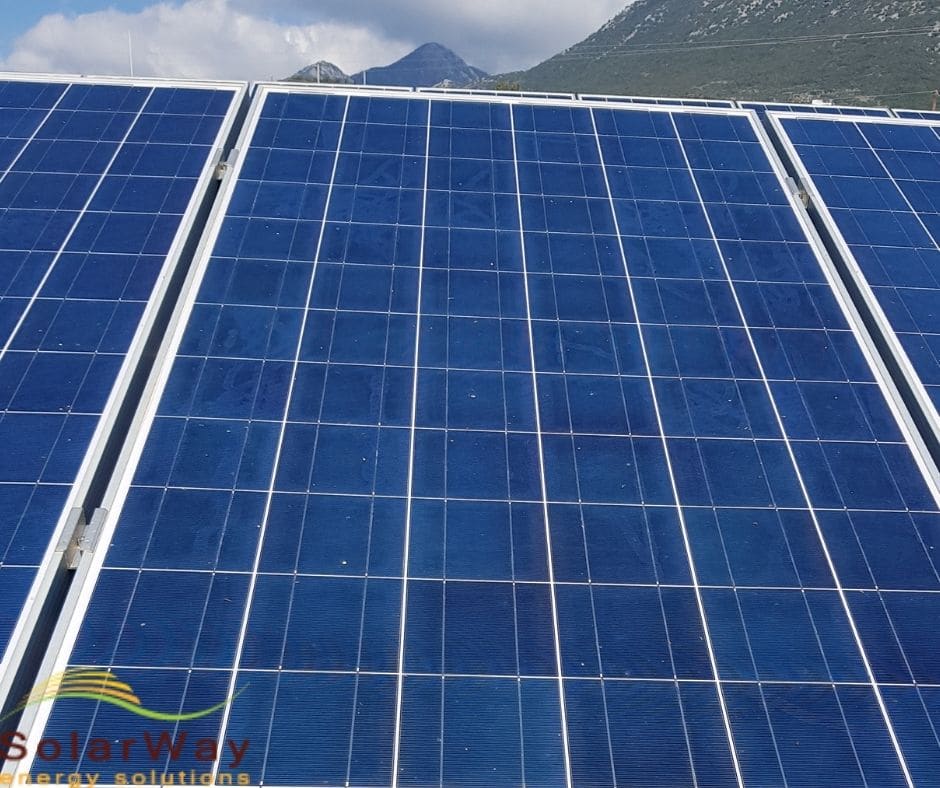
Figure 1 : Typical photos of solar panels affecetd by snail trail (from maintenace of photovoltaics parks of SolarWay)
Within a few years this kind of PV module defect became widespread. In 2012 it was reported that about 50% of all newly installed modules were more or less affected from “snail trails” [2]. The concern about the impact to module performance and possible long-term effects initiated a lot of scientific studies on the root cause of “snail trails”. This article gives an overview of what is known meanwhile about the mechanism of “snail trail” formation and what PV operators and manufacturers can derive from this knowledge.
The microstructure of “snail trail” discoloration
It became obvious by simple microscopic inspection of snail trail-affected module sites that the visual impression of dark stripes on the cell surface is caused by partially discoloured contact fingers. As ilustrated in fure 2, the impression of a homogeneous dark area is a kind of optical illusion since it is solely caused by a discontinuous brownish discoloration of the silver grid fingers but not the cell surface itself. Based on this very early finding it was suggested by some authors to replace the misleading initial name by the more correct name “grid finger discoloration”. However, this has not been generally accepted by the PV community.

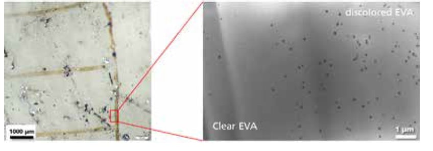
Further analysis of the origin of brownish grid finger discoloration required a skilled sample preparation and high resolution techniques. By detaching the glass and encapsulating EVA layer from a discoloured module area it was found that the brownish traces are located within the covering EVA very near to the cell/EVA interface [3]. Finally, it was found by transmission electron microscopy that the brownish colour within the EVA material correlates with the appearance of nanometre-sized particles (figure 3) A chemical analysis of those nanoparticles revealed silver as their main component. Thus, it could be concluded that the formation of silver nanoparticles within the EVA layer right above a contact finger is the microstructural and chemical reason for the visual impression of discoloured cell areas
The mechanism of “snail trail” formation
After having discovered silver nanoparticles as the microscopic origin of the grid finger discoloration the questions arise why and how they occur specifically at the sites of dark stripes or frames. One plausible explanation is supported by the observation that those grid finger discolorations which cross the cell strongly coincide with cell cracks. This is illustrated in Figure 4.

The electroluminescence EL image shows that the cell has a characteristic pattern of cracks. This pattern is completely identical to the pattern of the discoloration seen at the photograph of the same solar cell. This coincidence was found for all investigated samples with cell-crossing discoloration stripes and was reported by many authors. However, there is certain confusion with the definition of cracks and micro-cracks. Cracks which are related to grid finger discoloration as described above are always macroscopic cracks which penetrate the whole cell. This means they are 180-200 μm in vertical dimension (the whole wafer thickness) and several millimetres up to centimetres in lateral dimension. Micro-cracks are clearly different in their dimensions (some micrometres in depth) and occur for example as surface damage after wafer sawing. These terms should not be mixed up. The second form of grid finger discoloration, called framing, is located at the edges of the cell. Thus, the discoloration is correlated either to cell cracks or to the cell edges. Therefore, the probable reason for the onset of grid finger discoloration is moisture entering the PV module from the backside (through the back sheet) and entering the sunny side of the cell through cell cracks or between single cells. This assumption is supported by the observation that glass-glass modules seem to be completely resistant against grid finger discoloration, since the glass at the backside is a much better barrier to moisture than usual back sheet foils. After the invading water has entered the cell surface, a small fraction of silver from the grid fingers may dissolve and migrate into the encapsulation foil on top of the grid fingers. Through a chemical reaction the dissolved silver ions are reduced and form metallic nanoparticles exhibiting a typical brownish colour. It could be shown, that there is a correlation between the type of polymer foils used for module assembly and the sensitivity to grid finger discoloration [4]. Thus, the current hypothesis is that certain polymer foil additives trigger the formation of “snail trails” in photovoltaic modules, but this has not yet been investigated in detail.
It should be mentioned here, that there are controversial analytical results and conclusions concerning the chemical composition of “snail trail” discoloration. Mainly using Raman spectroscopy as the analytical method, a variety of silver compounds were found and attributed to the origin of “snail trails”. This includes silver acetate, silver carbonate, silver phosphate or silver sulphide [5, 6]. Possibly, there are different forms of grid finger discoloration and the term “snail trails” describes a class of failures. Nevertheless, it is commonly accepted that invading moisture plays a key role and that there is a dependency on the type of encapsulation and back sheet material. Further stress factors, like UV irradiation, current or temperature may be additional triggering factors. In our opinion this disunity of the scientists does not have any practical relevance, as discussed below.
Diagnostic test procedures for grid finger discoloration
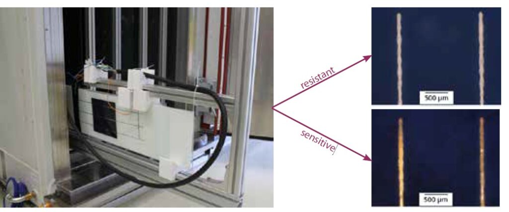
Several lab procedures have been developed to test the sensitivity of module materials for grid finger discoloration. This can be done by treatment of a one-cell mini-module with damp heat conditions under bias and subsequent microscopic inspection of grid fingers at the cell edge. As shown in Figure 5, a clear difference can be observed between samples which are sensitive to or resistant against grid finger discoloration after damp-heat treatment for 1,000 hours. In this example, the samples were different only in their foil materials (encapsulant and back sheet) but contained the same type of cell. This shows that the solar cell itself or the type of silver paste is of minor influence. The mini-module test is very useful for module manufacturers in order to qualify their foil materials with respect to grid finger discoloration. Therefore, there is an actual SEMI activity to standardise this kind of test (SEMI SNARF Document #6071). Unfortunately, this test principle is not fully applicable for standard-sized modules. It turned out in experiments that for standard modules not all sensitive material combinations showed grid finger discoloration after 1,000 hours of damp-heat testing. Probably, the test time is too short for big samples.
Studies had shown that the susceptibility of modules to grid finger discoloration is not tested by the IEC 61215 and a combined mechanical load, humidity freeze and UV test had been proposed [12]. For “snail trail” evaluation of installed PV modules the only straightforward test procedure is an electroluminescence measurement to detect cell cracks combined with microscopic inspection of grid fingers. This requires field inspection with mobile electroluminescence and microscopy equipment or in case of ambiguity the dismounting of the affected module and transportation into a PV service lab.
The impact of “snail trails” on module performance
From the microstructural origin of grid finger discoloration as described above, there is one major implication to its impact on the electrical module performance: the discoloured area is exclusively at the site of grid fingers, not on the cell surface itself. Therefore, the active cell surface is not impaired and, hence, the discoloration does not lead to reduced light harvesting. Furthermore, electron microscopic studies on affected grid fingers showed that there is no significant change of material structure or cross section which might have influence to the conductivity [5]. Thus, “snail trails” themselves should not cause a reduction of electrical performance. In practice, this has been investigated at different places and published several times [6-8]. At first glance, many examples for reduced power output from “snail trail” affected PV modules have been found. However, it turned out that it is difficult to measure the influence of grid finger discolouration separately from any underlying cell cracks.
An extreme example is shown in Figure 6. A section of a PV module is shown which is significantly affected from “snail trails”. The comparison between photograph and electroluminescence image confirms that each dark trace is correlated to a cell crack. In this case however, so many cracks have formed that many cell areas became electrically isolated and hence, were lost for the module’s performance. In this case, one can even compare it quantitatively: the measured reduction in power output was ~40% which matches almost exactly the sum of inactive cell area. Besides those extreme cases, it was confirmed also for modules with little or moderate discoloration that the power reduction (if any) is assigned to the cell cracks and not to the grid finger discoloration as such [8, 12].

Generally, it is important to minimise the number of macroscopic cracks already in the cell and module production. However, not every crack immediately leads to a power loss and one has to distinguish between electrically active and inactive cracks. Active cracks cause electrically isolated cell areas and result in a power loss which is detectable in the standard sun-simulator test. On the other hand, inactive cracks hardly affect cell or module power but can become electrically active later on during the module operation in the field.
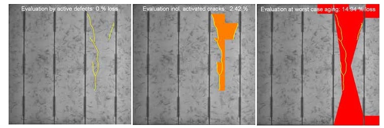
EL imaging is a commonly applied method for crack detection in the PV industry. As a manual operator-based EL inspection depends on the operator’s experience and skills it is of limited reliability and can hardly be used to obtain quantitative results. Therefore, the method of choice is a fully automated EL inspection, which includes automated software algorithms in order to detect nearly all macroscopic cracks timely during cell and module production. Applying modern image processing algorithms, it is not only possible to detect the smallest cracks reliably; the prospective power loss can also be predicted by software simulation, assuming that the inactive cracks become active later on in the field (see Figure 7). An automatic EL inspection in module production right before lamination enables the replacement of defective cells and avoids both “snail trails” and, even worse, cracks which will cause power loss in the module.
“Snail trails” and long-term reliability of modules
Only recently, the first studies on the mid-term evolution of grid finger discoloration have been published [9]. The authors investigated modules affected by “snail trails” over the period of two years and came to the conclusion that after the initial formation of discoloration in the first year no (or only very little) evolution of new traces could be detected two years later.
Moreover, no further decrease of electrical performance was observed. Thus, the good news is that “snail trails” obviously develop only at the beginning of outdoor operation and do not have any measurable long-term impact. One can even regard “snail trails” as indicator of cell cracks which were invisible otherwise. Having in mind that cell cracks may cause severe power loss and that those cracks may be the starting point for dramatic cell damage after mechanical stress like snow or typhoon, “snail trails” may serve the PV operator as guide for regular inspection.
References
1] M. Kφntges, I. Kunze, V. Naumann, S. Richter, C. Hagendorf, Schneckenspuren, Snail Tracks, Worm Marks und Mikrorisse, 8. Modulworkshop, TάV Rheinland (2011)
[2] Joachim Treder, 9. Workshop „Photovoltaik- Modultechnik“ TάV Rheinland 2012
[3] Meyer, S.; Timmel, S.; Richter, S.; Werner, M.; Glδser, M.; Swatek, S.; Braun, U.; Hagendorf, C., Silver nanoparticles cause snail trails in photovoltaic modules, Solar Energy Materials & Solar Cells 121(2014)171–175.
[4] Meyer, S.; Timmel, S.; Glδser, M.; Braun, U.; Wachtendorf, V.; Hagendorf, C., Polymer foil additives trigger the formation of snail trails in photovoltaic modules, Solar Energy Materials & Solar Cells 130 (2014) 64–70.
[5] Peng, P., Hu, A.M., Zheng, W.D., Su, P., He, D., Oakes, K.D., Fu, A., Han, R.J., Lee, S.L., Tang, J. and Zhou, Y.N., Microscopy study of snail trail phenomenon on photovoltaic modules, RSC Advances 2012; 2: 11359-11365.
[6] Duerr I Bierbaum J Metzger J Richter J Philipp D, Silver Grid Finger Corrosion on Snail Track affected PV Modules – Investigation on Degradation Products and Mechanisms, Energy Procedia, 2016 vol: 98 pp: 74-85
[7] S. Richter, M. Werner, S. Swatek, C. Hagendorf, Understanding the Snail Trail Effect in Silicon Solar Modules on Microstructural Scale, 27th European Photovoltaic Solar Energy Conference and Exhibition, 24-28 September 2012, Frankfurt/Main, Germany
[8] Yang H Chang J Wang H Song D, Power Degradation Caused by Snail Trails in Urban Photovoltaic Energy Systems, Energy Procedia, 2016 vol: 88 pp: 422-428.
[9] A. Dolara and S. Leva and G. Manzolini and E. Ogliari, Investigation on Performance Decay on Photovoltaic Modules: Snail Trails and Cell Microcracks, IEEE Journal of Photovoltaics, 2014, vol: 4 pp: 1204-1211.
[10] Han-Chang Liu, Chung-Teng Huang, Wen- Kuei Lee, Shih-Siang Yan, Fu-Ming Lin, A Defect Formation as Snail Trails in Photovoltaic Modules, Energy and Power Engineering, 2015, 7, 348-353
[11] A. Dolara and G. C. Lazaroiu and S. Leva and G. Manzolini and L. Votta, Snail Trails and Cell Microcrack Impact on PV Module Maximum Power and Energy Production, IEEE Journal of Photovoltaics, 2016, vol: 6, pp: 1269-1277.
[12] J. Berghold, M. Roericht, A. Bφttcher, S. Wendlandt, M. Hanusch, S. Koch, P. Grunow and B. Stegemann “Electrochemical corrosion within solar panels” 27th EUPVSEC (2012) 3511-3517

